LMK04806BISQE/NOPB点击型号即可查看芯片规格书
LMK04806BISQE/NOPB 中文资料规格参数
| 技术参数 | 频率 | 500 MHz |
电源电压(DC) | 3.15V (min) | |
输出接口数 | 12 | |
电路数 | 1 | |
针脚数 | 64 | |
占空比 | 50 % | |
工作温度(Max) | 85 ℃ | |
工作温度(Min) | -40 ℃ | |
电源电压 | 3.15V ~ 3.45V | |
电源电压(Max) | 3.45 V | |
电源电压(Min) | 3.15 V | |
| 封装参数 | 安装方式 | Surface Mount |
引脚数 | 64 | |
封装 | WQFN-64 | |
| 外形尺寸 | 长度 | 9 mm |
宽度 | 9 mm | |
高度 | 0.8 mm | |
封装 | WQFN-64 | |
| 物理参数 | 工作温度 | -40℃ ~ 85℃ |
| 其他 | 产品生命周期 | Active |
包装方式 | Tape & Reel (TR) | |
| 符合标准 | RoHS标准 | RoHS Compliant |
含铅标准 | Lead Free | |
REACH SVHC版本 | 2015/06/15 | |
| 海关信息 | ECCN代码 | EAR99 |
LMK04806BISQE/NOPB 引脚图 | 封装图 | 封装焊盘图
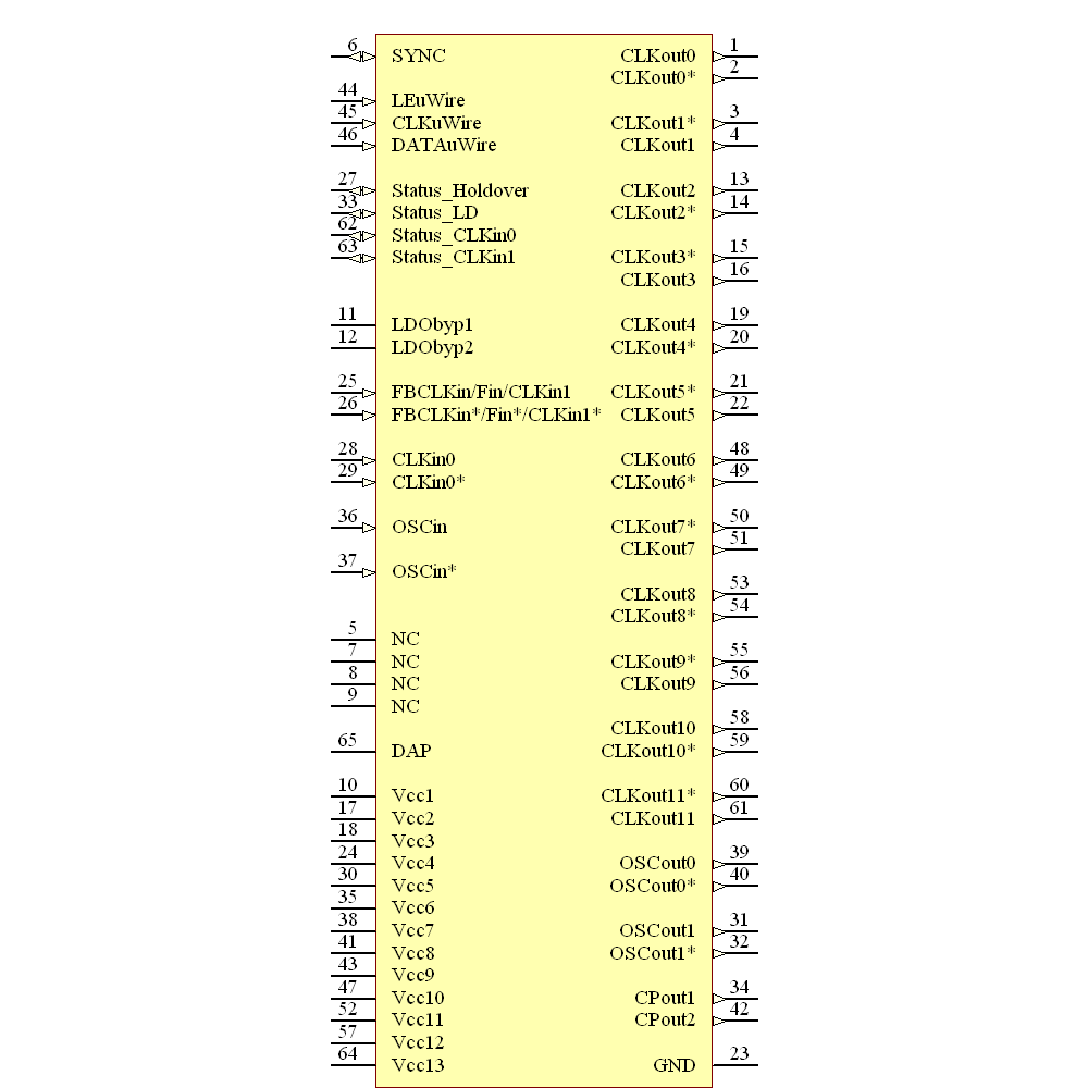
LMK04806BISQE/NOPB 引脚图
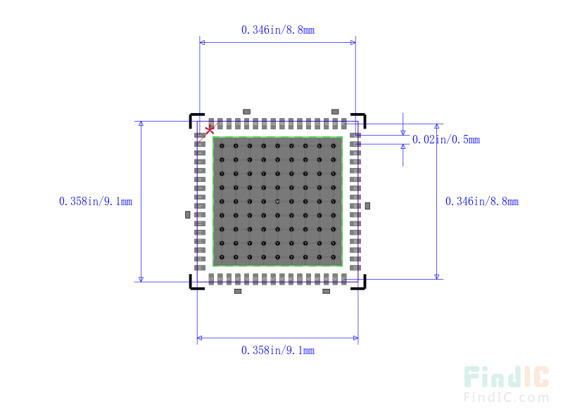
LMK04806BISQE/NOPB 封装图
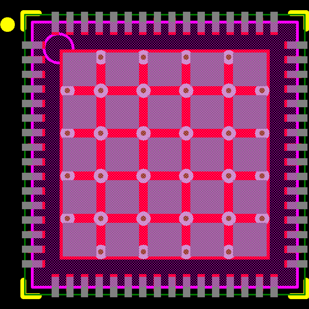
LMK04806BISQE/NOPB 封装焊盘图
产品概述
时钟发生器, 抖动滤除器, 500MHZ, 3.15 V至3.45 V, 12输出, WQFN-64
TheLMK04806BISQE/NOPBis a highest-performance Clock Conditioner with superior clock jitter cleaning, generation and distribution with advanced features to meet next generation system requirements. The dual loop PLLatinum architecture is capable of 111fs RMS jitter (12kHz to 20MHz) using a low noise VCXO module or sub-200fs RMS jitter (12kHz to 20MHz) using an external crystal and varactor diode. The dual loop architecture consists of two high-performance phase-locked loops (PLL), a low-noise crystal oscillator circuit and a high-performance voltage controlled oscillator (VCO). The first PLL (PLL1) provides low-noise jitter cleaner functionality while the second PLL (PLL2) performs the clock generation. PLL1 can be configured to either work with an external VCXO module or the integrated crystal oscillator with an external tuneable crystal and varactor diode.
.Ultra-low RMS jitter performance
.Dual loop PLLatinum™ PLL architecture
.Integrated low-noise crystal oscillator circuit
.Holdover mode when input clocks are lost
.Automatic or manual triggering/recovery
.2 Redundant input clocks with LOS
.12 LVPECL, LVDS or LVCMOS Programmable outputs
.Digital delay - Fixed or dynamically adjustable
.25ps Step analogue delay control
.Three default clock outputs at power up
.Multi-mode - Dual PLL, single PLL and clock distribution
.Green product and no Sb/Br
Device has limited built-in ESD protection. The leads should be shorted together or the device placed in conductive foam during storage or handling to prevent electrostatic damage to the MOS gates.
