SN74LV595APWT点击型号即可查看芯片规格书
SN74LV595APWT 中文资料规格参数
| 技术参数 | 频率 | 170 MHz |
电源电压(DC) | 2.00V ~ 5.50V | |
输出接口数 | 9 | |
针脚数 | 16 | |
位数 | 8 | |
电压波节 | 5.00 V, 3.30 V, 2.50 V | |
输出电流驱动 | -1.00 mA | |
输入数 | 1 | |
工作温度(Max) | 85 ℃ | |
工作温度(Min) | -40 ℃ | |
电源电压 | 2V ~ 5.5V | |
电源电压(Max) | 5.5 V | |
电源电压(Min) | 2 V | |
| 封装参数 | 安装方式 | Surface Mount |
引脚数 | 16 | |
封装 | TSSOP-16 | |
| 外形尺寸 | 封装 | TSSOP-16 |
| 物理参数 | 工作温度 | -40℃ ~ 85℃ |
| 其他 | 产品生命周期 | Active |
包装方式 | Tape & Reel (TR) | |
制造应用 | 电源管理, 通信与网络, 计算机和计算机周边 | |
| 符合标准 | RoHS标准 | RoHS Compliant |
含铅标准 | Lead Free | |
REACH SVHC标准 | No SVHC | |
REACH SVHC版本 | 2015/06/15 | |
| 海关信息 | ECCN代码 | EAR99 |
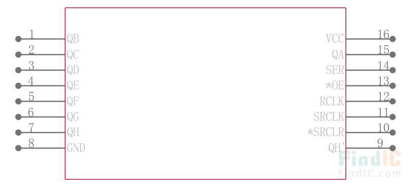
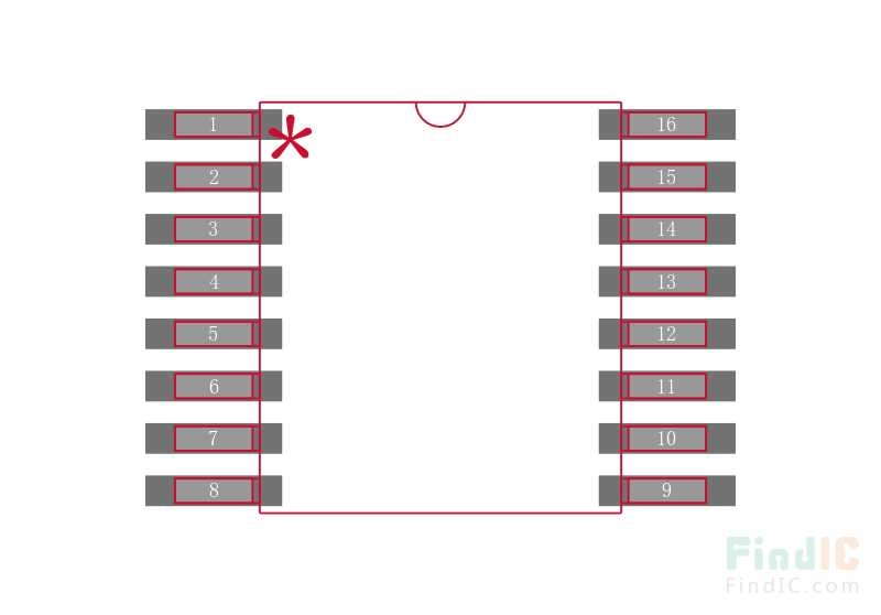
SN74LV595APWT 引脚图 | 封装图 | 封装焊盘图

SN74LV595APWT 引脚图

SN74LV595APWT 封装图

SN74LV595APWT 封装焊盘图
产品概述
TEXAS INSTRUMENTS SN74LV595APWT 移位寄存器, LV系列, 串行至并行, 1元件, TSSOP, 16 引脚, 2 V, 5.5 V
TheSN74LV595APWTis a 8-bit serial-in parallel-out Shift Register feeds an 8-bit D-type storage register. The storage register has parallel 3-state outputs. Separate clocks are provided for the shift and storage registers. The shift register has a direct overriding clear (SRCLR\\) input, serial (SER) input and serial outputs for cascading. When the OE\ input is high, the outputs are in the high-impedance state. Both the shift register clock (SRCLK) and storage register clock (RCLK) are positive-edge triggered. If both clocks are connected together, the shift register always is one clock pulse ahead of the storage register. This low-drive CMOS device can be used for a multitude of bus interface type applications where output ringing is a concern. The low drive and slow edge rates will minimize overshoot and undershoot on the outputs. The inputs are 5V tolerant allowing for down translation to VCC.
.Support mixed-mode voltage operation on all ports
.Ioff Supports live insertion, partial power-down mode and back-drive protection
.Shift register has direct clear
.Latch-up performance exceeds 250mA per JESD 17
.Green product and no Sb/Br