TLV2322ID 中文资料规格参数
| 技术参数 | 输出电流 | ≤30 mA |
供电电流 | 20 µA | |
电路数 | 2 | |
通道数 | 2 | |
耗散功率 | 725 mW | |
共模抑制比 | 65dB ~ 94dB | |
输入补偿漂移 | 1.10 µV/K | |
带宽 | 27 kHz | |
转换速率 | 30.0 mV/μs | |
增益频宽积 | 0.085 MHz | |
输入补偿电压 | 1.1 mV | |
输入偏置电流 | 0.0000006μA @5V | |
工作温度(Max) | 85 ℃ | |
工作温度(Min) | -40 ℃ | |
增益带宽 | 85 kHz | |
耗散功率(Max) | 725 mW | |
共模抑制比(Min) | 65 dB | |
电源电压 | 2V ~ 8V | |
电源电压(Max) | 8 V | |
电源电压(Min) | 2 V | |
| 封装参数 | 安装方式 | Surface Mount |
引脚数 | 8 | |
封装 | SOIC-8 | |
| 外形尺寸 | 长度 | 4.9 mm |
宽度 | 3.91 mm | |
高度 | 1.58 mm | |
封装 | SOIC-8 | |
| 物理参数 | 工作温度 | -40℃ ~ 85℃ |
| 其他 | 产品生命周期 | Active |
包装方式 | Tube | |
| 符合标准 | RoHS标准 | RoHS Compliant |
含铅标准 | Lead Free | |
REACH SVHC标准 | No SVHC | |
REACH SVHC版本 | 2015/06/15 |
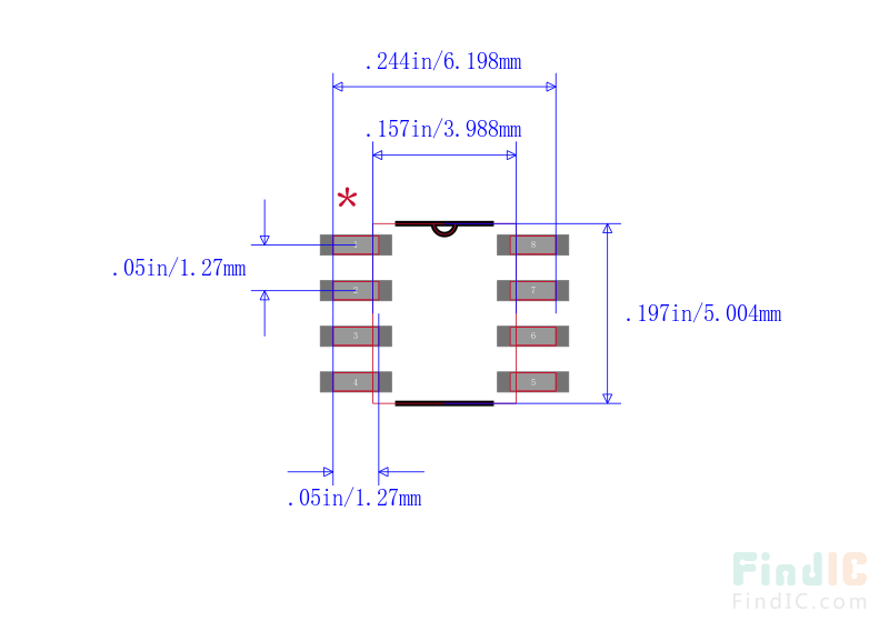
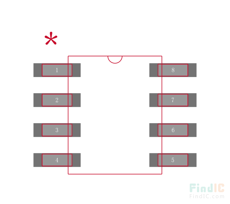
TLV2322ID 封装图 | 封装焊盘图

TLV2322ID 封装图

TLV2322ID 封装焊盘图
产品概述
LinCMOSE低电压低功耗运算放大器 LinCMOSE LOW-VOLTAGE LOW-POWER OPERATIONAL AMPLIFIERS
description
The TLV232x operational amplifiers are in a family of devices that has been specifically designed for use in low-voltage single-supply applications. This amplifier is especially well suited to
ultra-low-power systems that require devices to consume the absolute minimum of supply
currents. Each amplifier is fully functional down to a minimum supply voltage of 2 V, is fully
characterized, tested, and specified at both 3-V and 5-V power supplies. The common-mode input
voltage range includes the negative rail and extends to within 1 V of the positive rail.
Wide Range of Supply Voltages Over Specified Temperature Range:
TA= –40°C to 85°C...2 V to 8 V
Fully Characterized at 3 V and 5 V
Single-Supply Operation
Common-Mode Input Voltage Range
Extends Below the Negative Rail and up to VDD –1 V at TA= 25°C
Output Voltage Range Includes Negative Rail
High Input Impedance...1012 Ω Typical
ESD-Protection Circuitry
Designed-In Latch-Up Immunity