NB100LVEP221MNG点击型号即可查看芯片规格书
NB100LVEP221MNG 中文资料规格参数
| 技术参数 | 无卤素状态 | Halogen Free |
电路数 | 1 | |
最大占空比 | 50.5 % | |
工作温度(Max) | 85 ℃ | |
工作温度(Min) | -40 ℃ | |
电源电压 | 2.375V ~ 3.8V | |
| 封装参数 | 安装方式 | Surface Mount |
引脚数 | 52 | |
封装 | QFN-52 | |
| 外形尺寸 | 封装 | QFN-52 |
| 物理参数 | 工作温度 | -40℃ ~ 85℃ |
| 其他 | 产品生命周期 | Active |
包装方式 | Tray | |
制造应用 | Multiple Clock Sources | |
| 符合标准 | RoHS标准 | RoHS Compliant |
含铅标准 | Lead Free | |
| 海关信息 | ECCN代码 | EAR99 |
NB100LVEP221MNG 引脚图 | 封装图 | 封装焊盘图
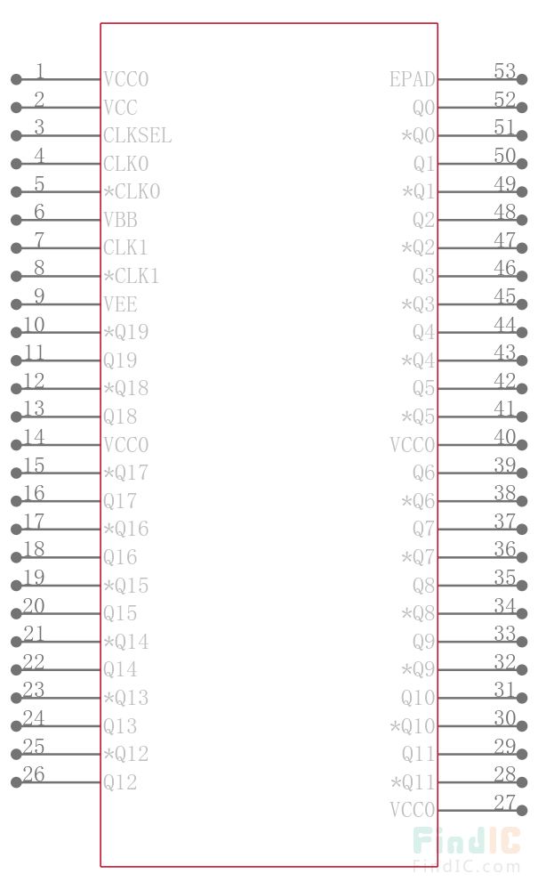
NB100LVEP221MNG 引脚图

NB100LVEP221MNG 封装图
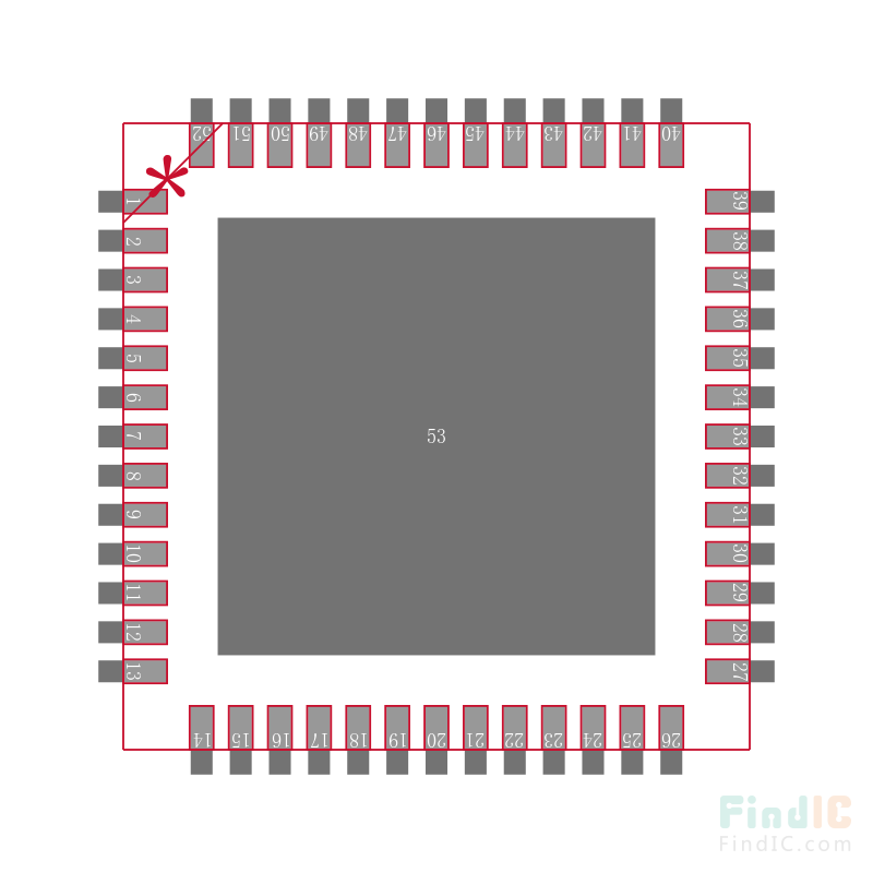
NB100LVEP221MNG 封装焊盘图
产品概述
Clock Multiplexer 20Out 2IN 1:20 52Pin QFN EP Tray
The NB100LVEP221 is a low skew 2:1:20 differential driver, designed with clock distribution in mind, accepting two clock sources into an input multiplexer. The two clock inputs are differential ECL/PECL; CLK1/CLK1bar can also receive HSTL signal levels. The LVPECL input signals can be either differential or single-ended (if the VThe LVEP221 specifically guarantees low output-to-output skew. Optimal design, layout, and processing minimize skew within a device and from device to device.To ensure tightest skew, both sides of differential outputs should be terminated identically into 50 ohms even if only one output is being used. If an output pair is unused, both outputs may be left open (unterminated) without affecting skew.The NB100LVEP221, as with most other ECL devices, can be operated from a positive V supply in LVPECL mode. This allows the LVEP221 to be used for high performance clock distribution in +3.3 V or +2.5 V systems. In a PECL environment, series or Thevenin line terminations are typically used as they require no additional power supplies. For more information on PECL terminations, designers should refer to Application Note AND8020/D. pin, an internally generated voltage supply, is available to this device only. For single-ended LVPECL input conditions, the unused differential input is connected to V as a switching reference voltage. V may also rebias AC coupled inputs. When used, decouple V via a 0.01 uF capacitor and limit current sourcing or sinking to 0.5 mA. When not used, VSingle-ended CLK input operation is limited to V >/= 3.0 V in LVPECL mode, or V
Features
---
|
.15 ps Typical Output-to-Output Skew
.40 ps Typical Device-to-Device Skew
.Jitter Less than 2 ps RMS
.Maximum Frequency > 1.0 Ghz Typical
.VBB Output
.540 ps Typical Propagation Delay
.LVPECL and HSTL Mode Operating Range: VCC = 2.375 V to 3.8 V with VEE = 0 V
.NECL Mode Operating Range: VCC = 0 V with VEE = -2.375 V to -3.8 V
.Q Output will Default Low with Inputs Open or at VEE
