ADG736BRM点击型号即可查看芯片规格书
ADG736BRM 中文资料规格参数
| 技术参数 | 输出接口数 | 4 |
触点类型 | SPDT | |
供电电流 | 1 nA | |
电路数 | 2 | |
通道数 | 2 | |
位数 | 2 | |
耗散功率 | 0.315 W | |
输入数 | 2 | |
工作温度(Max) | 125 ℃ | |
工作温度(Min) | -40 ℃ | |
3dB带宽 | 200 MHz | |
耗散功率(Max) | 315 mW | |
电源电压(Max) | 5.5 V | |
电源电压(Min) | 1.8 V | |
| 封装参数 | 安装方式 | Surface Mount |
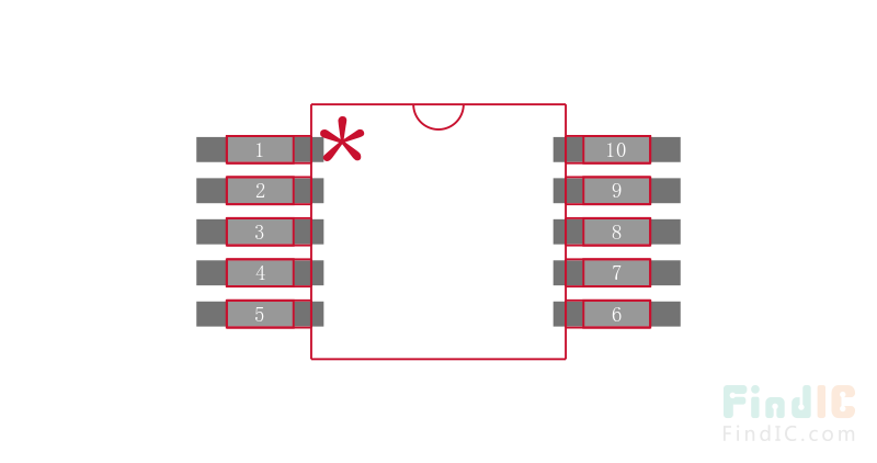
引脚数 | 10 | |
封装(公制) | SOP | |
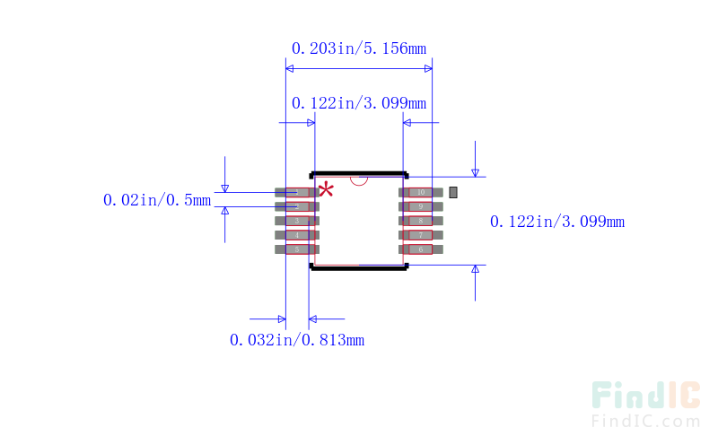
封装 | MSOP-10 | |
| 外形尺寸 | 长度 | 3 mm |
宽度 | 3 mm | |
高度 | 0.85 mm | |
封装(公制) | SOP | |
封装 | MSOP-10 | |
| 物理参数 | 工作温度 | -40℃ ~ 125℃ (TA) |
| 其他 | 产品生命周期 | Active |
包装方式 | Tube | |
| 符合标准 | RoHS标准 | Non-Compliant |
含铅标准 | Contains Lead | |
| 海关信息 | ECCN代码 | EAR99 |
香港进出口证 | NLR |
ADG736BRM 引脚图 | 封装图 | 电路图 | 封装焊盘图

ADG736BRM 引脚图
ADG736BRM 封装图

ADG736BRM 电路图
ADG736BRM 封装焊盘图
产品概述
CMOS低电压4欧姆双通道单刀双掷开关 CMOS Low Voltage 4 ohm Dual SPDT Switch
Product Details
The ADG736 is a monolithic device comprising two independently selectable CMOS single pole, double throw (SPDT) switches. These switches are designed using a submicron process that provides low power dissipation yet gives high switching speed, low on resistance, low leakage currents, and wide input signal bandwidth.
The on resistance profile is very flat over the full analog signal range. This ensures excellent linearity and low distortion when switching audio signals. Fast switching speed also makes the part suitable for video signal switching.
The ADG736 operates from a single 1.8 V to 5.5 V supply, making it ideally suited to portable and battery-powered instruments.
Each switch conducts equally well in both directions when on, and each has an input signal range that extends to the power supplies. The ADG736 exhibits break-before-make switching action.
The ADG736 is available in a 10-lead MSOP package.
**Product Highlights**
.1.8 V to 5.5 V Single-Supply Operation. The ADG736 offers high performance, including low on resistance and fast switching times. It is fully specified and guaranteed with 3 V and 5 V supply rails.
.Very Low RON (4.5 Ω Maximum at 5 V, 8 Ω Maximum at 3 V). At a supply voltage of 1.8 V, RON is typically 35 Ω over the temperature range.
.Low On Resistance Flatness.
.−3 dB Bandwidth > 200 MHz.
.Low Power Dissipation. CMOS construction ensures low power dissipation.
.Fast tON/tOFF.
.Break-Before-Make Switching Action.
.10-Lead MSOP Package.
**
**Applications**
**
.USB 1.1 signal switching circuits
.Cell phones
.PDAs
.Battery-powered systems
.Communications systems
.Sample-and-hold systems
.Audio signal routing
.Audio and video switching
.Mechanical reed relay replacement
### Features and Benefits
.1.8 V to 5.5 V single supply
.Automotive temperature range: −40°C to +125°C
.2.5 Ω (typical) on resistance
.Low on resistance flatness
.−3 dB bandwidth > 200 MHz
.Rail-to-rail operation10-lead
.MSOP package
.Fast switching times
TON 16 ns
TOFF 8 ns
.Typical power consumption (<0.01 μW)
.TTL-/CMOS-compatible
.Qualified for automotive applications
