AD620AN点击型号即可查看芯片规格书
AD620AN 中文资料规格参数
| 技术参数 | 供电电流 | 900 µA |
电路数 | 1 | |
通道数 | 1 | |
耗散功率 | 0.65 W | |
共模抑制比 | 73 dB | |
带宽 | 1.00 MHz | |
转换速率 | 1.20 µV/μs | |
输入补偿电压 | 30 µV | |
输入偏置电流 | 500 pA | |
工作温度(Max) | 85 ℃ | |
工作温度(Min) | -40 ℃ | |
3dB带宽 | 1 MHz | |
增益带宽 | 73 dB | |
耗散功率(Max) | 650 mW | |
共模抑制比(Min) | 73 dB | |
电源电压(Max) | 30V ~ 50V | |
| 封装参数 | 安装方式 | Through Hole |
引脚数 | 8 | |
封装 | PDIP-8 | |
| 外形尺寸 | 宽度 | 6.35 mm |
高度 | 3.3 mm | |
封装 | PDIP-8 | |
| 物理参数 | 工作温度 | -40℃ ~ 85℃ |
| 其他 | 产品生命周期 | Active |
包装方式 | Tube | |
制造应用 | ECG Patient Monitoring, Body Composition Measurement, Health, Wellness and Fitness, Clinical Monitoring, Respiration Measurement, EEG Measurement, Healthcare | |
| 符合标准 | RoHS标准 | Non-Compliant |
含铅标准 | PB free | |
| 海关信息 | 香港进出口证 | NLR |
AD620AN 引脚图 | 封装图 | 电路图 | 封装焊盘图
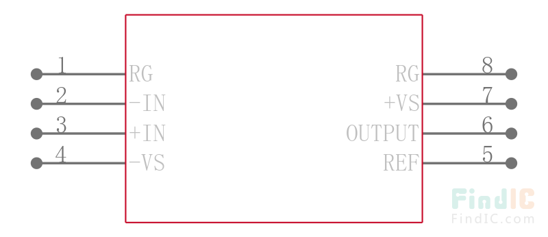
AD620AN 引脚图
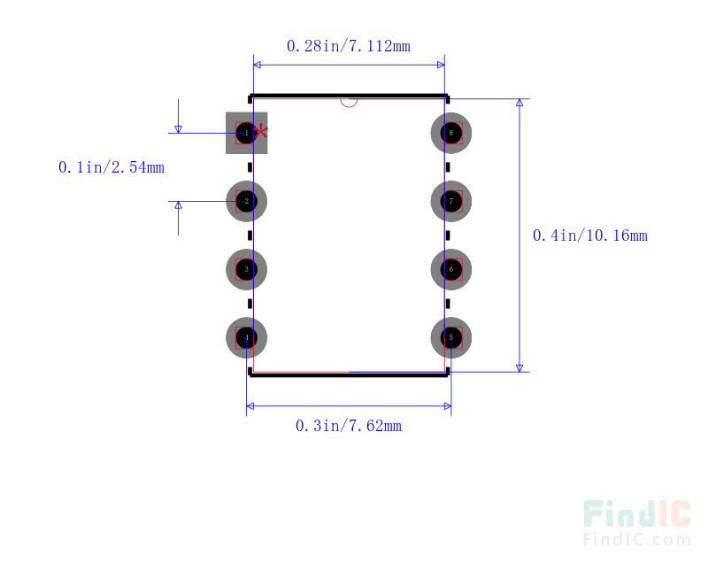
AD620AN 封装图
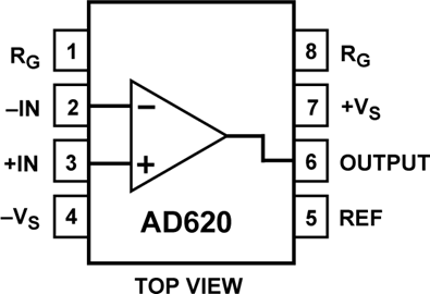
AD620AN 电路图
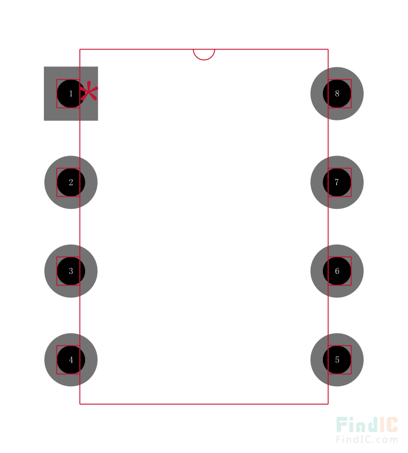
AD620AN 封装焊盘图
产品概述
低成本低功耗仪表放大器 Low Cost Low Power Instrumentation Amplifier
Product Details
The AD620 is a low cost, high accuracy instrumentation amplifier that requires only one external resistor to set gains of 1 to 10,000. Furthermore, the AD620 features 8-lead SOIC and DIP packaging that is smaller than discrete designs and offers lower power (only 1.3 mA max supply current), making it a good fit for battery powered, portable (or remote) applications.
The AD620, with its high accuracy of 40 ppm maximum nonlinearity, low offset voltage of 50 µV max, and offset drift of 0.6 µV/°C max, is ideal for use in precision data acquisition systems, such as weigh scales and transducer interfaces. Furthermore, the low noise, low input bias current, and low power of the AD620 make it well suited for medical applications such as ECG and noninvasive blood pressure monitors.
The low input bias current of 1.0 nA max is made possible with the use of Superϐeta processing in the input stage. The AD620 works well as a preamplifier due to its low input voltage noise of 9 nV/√Hz at 1 kHz, 0.28 μV p-p in the 0.1 Hz to 10 Hz band, and 0.1 pA/√Hz input current noise. Also, the AD620 is well suited for multiplexed applications with its settling time of 15 μs to 0.01%, and its cost is low enough to enable designs with one in-amp per channel.
### Features and Benefits
.EASY TO USE
Gain Set with One External Resistor
(Gain Range 1 to 10,000)
Wide Power Supply Range (±2.3 V to ±18 V)
Higher Performance than Three
Op Amp IA Designs
Available in 8-Lead DIP and SOIC Packaging
Low Power, 1.3 mA max Supply
.LOW NOISE
9 nV/√Hz, @ 1 kHz, Input Voltage Noise
0.28 µV p-p Noise (0.1 Hz to 10 Hz)
.EXCELLENT DC PERFORMANCE (B GRADE)
50 µV max, Input Offset Voltage
0.6 µV/°C max, Input Offset Drift
1.0 nA max, Input Bias Current
100 dB min Common-Mode
Rejection Ratio (G = 10)
.EXCELLENT AC SPECIFICATIONS
120 kHz Bandwidth (G = 100)
15 µs Settling Time to 0.01%
