AD9516-1BCPZ点击型号即可查看芯片规格书
AD9516-1BCPZ 中文资料规格参数
| 技术参数 | 频率 | 2.65 GHz |
电源电压(DC) | 3.13V (min) | |
输出接口数 | 14 | |
电路数 | 1 | |
针脚数 | 64 | |
工作温度(Max) | 85 ℃ | |
工作温度(Min) | -40 ℃ | |
电源电压 | 3.135V ~ 3.465V | |
电源电压(Max) | 3.465 V | |
电源电压(Min) | 3.135 V | |
| 封装参数 | 安装方式 | Surface Mount |
引脚数 | 64 | |
封装 | LFCSP-64 | |
| 外形尺寸 | 长度 | 9 mm |
宽度 | 9 mm | |
高度 | 0.83 mm | |
封装 | LFCSP-64 | |
| 物理参数 | 工作温度 | -40℃ ~ 85℃ |
| 其他 | 产品生命周期 | Active |
包装方式 | Tray | |
制造应用 | 传感与仪器, 无线, 时钟与计时 | |
| 符合标准 | RoHS标准 | RoHS Compliant |
含铅标准 | Lead Free | |
REACH SVHC版本 | 2015/12/17 | |
| 海关信息 | ECCN代码 | EAR99 |
AD9516-1BCPZ 引脚图 | 封装图 | 电路图 | 封装焊盘图
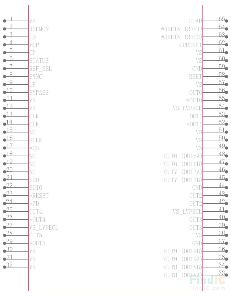
AD9516-1BCPZ 引脚图
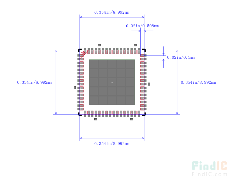
AD9516-1BCPZ 封装图
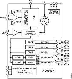
AD9516-1BCPZ 电路图
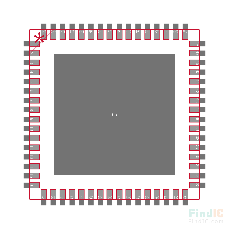
AD9516-1BCPZ 封装焊盘图
产品概述
ANALOG DEVICES AD9516-1BCPZ 芯片, 时钟发生器, 2.65GHZ, LFCSP-64
Product Details
The AD9516-11 provides a multi-output clock distribution function with subpicosecond jitter performance, along with an on-chip PLL and VCO. The on-chip VCO tunes from 2.30 GHz to 2.65 GHz. Optionally, an external VCO/VCXO of up to 2.4 GHz can be used.
The AD9516-1 emphasizes low jitter and phase noise to maximize data converter performance, and it can benefit other applications with demanding phase noise and jitter requirements.
The AD9516-1 features six LVPECL outputs (in three pairs) and four LVDS outputs (in two pairs). Each LVDS output can be reconfigured as two CMOS outputs. The LVPECL outputs operate to 1.6 GHz, the LVDS outputs operate to 800 MHz, and the CMOS outputs operate to 250 MHz.
Each pair of outputs has dividers that allow both the divide ratio and coarse delay (or phase) to be set. The range of division for the LVPECL outputs is 1 to 32. The LVDS/CMOS outputs allow a range of divisions up to a maximum of 1024.
The AD9516-1 is available in a 64-lead LFCSP and can be operated from a single 3.3 V supply. An external VCO, which requires an extended voltage range, can be accommodated by connecting the charge pump supply (VCP) to 5 V. A separate LVPECL power supply can be from 2.5 V to 3.3 V (nominal).
The AD9516-1 is specified for operation over the industrial range of −40°C to +85°C.
**Applications**
.Low jitter, low phase noise clock distribution
.10/40/100 Gb/sec networking line cards, including SONET, Synchronous Ethernet, OTU2/3/4
.Forward error correction (G.710)
.Clocking high speed ADCs, DACs, DDSs, DDCs, DUCs, MxFEs
.High performance wireless transceivers
.ATE and high performance instrumentation
1 AD9516 is used throughout to refer to all the members of the AD9516 family. However, when AD9516-1 is used, it is referring to that specific member of the AD9516 family.
### Features and Benefits
.Low phase noise, phase-locked loop (PLL)
\-- On-chip VCO tunes from 2.30 GHz to 2.65 GHz
\-- External VCO/VCXO to 2.4 GHz optional
\-- 1 differential or 2 single-ended reference inputs -- Reference monitoring capability
.**6 pairs of 1.6 GHz LVPECL outputs
**\-- Each output pair shares a 1-to-32 divider with coarse phase delay
\-- Additive output jitter:
225 fs rms
\-- Channel-to-channel skew paired outputs of <10 ps
.**4 pairs of 800 MHz LVDS clock outputs
**\-- Each output pair shares two cascaded 1-to-32 dividers with coarse phase delay
\-- Additive output jitter:
275 fs rms
.Each LVDS output can be reconfigured as two 250 MHz CMOS outputs
.Automatic synchronization of all outputs on power-up
.Manual output synchronization available
.64-lead LFCSP
.See datasheet for additional features
