SN74LV07ANSR 中文资料规格参数
| 技术参数 | 电源电压(DC) | 2.00V ~ 5.50V |
输出接口数 | 6 | |
通道数 | 6 | |
位数 | 6 | |
传送延迟时间 | 8.50 ns | |
电压波节 | 5.00 V, 3.30 V, 2.50 V | |
逻辑门数量 | 6 | |
输出电流驱动 | 16.0 mA | |
输入数 | 6 | |
工作温度(Max) | 125 ℃ | |
工作温度(Min) | -40 ℃ | |
电源电压 | 2V ~ 5.5V | |
电源电压(Max) | 5.5 V | |
电源电压(Min) | 2 V | |
| 封装参数 | 安装方式 | Surface Mount |
引脚数 | 14 | |
封装 | SOP-14 | |
| 外形尺寸 | 长度 | 10.3 mm |
宽度 | 5.3 mm | |
高度 | 1.95 mm | |
封装 | SOP-14 | |
| 物理参数 | 工作温度 | -40℃ ~ 125℃ (TA) |
| 其他 | 产品生命周期 | Active |
包装方式 | Tape & Reel (TR) | |
| 符合标准 | RoHS标准 | RoHS Compliant |
含铅标准 | Lead Free |
SN74LV07ANSR 引脚图 | 封装图 | 封装焊盘图
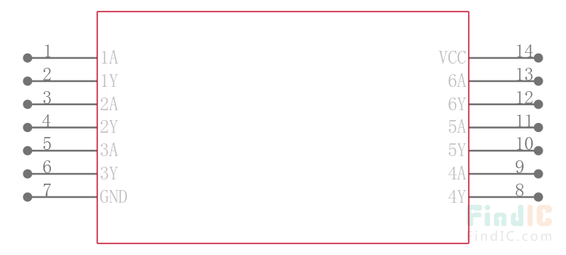
SN74LV07ANSR 引脚图

SN74LV07ANSR 封装图
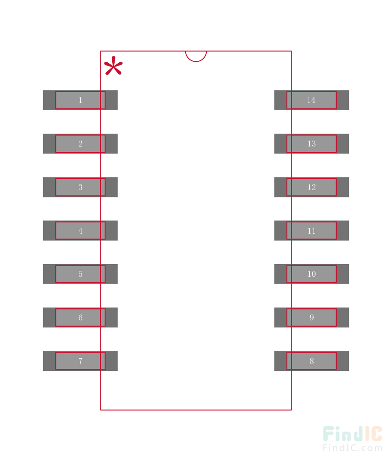
SN74LV07ANSR 封装焊盘图
产品概述
HEX缓冲器/带漏极开路输出驱动程序 HEX BUFFERS/DRIVERS WITH OPEN-DRAIN OUTPUTS
description/ordering information
These hex buffers/drivers are designed for 2-V to 5.5-V VCCoperation.
The ’LV07A devices perform the Boolean function Y = A in positive logic.
The open-drain outputs require pullup resistors to perform correctly and can be connected to other open-drain outputs to implement active-low wired-OR or active-high wired-AND functions.
2-V to 5.5-V VCCOperation
Typical VOLP(Output Ground Bounce) <0.8 V at VCC = 3.3 V, TA= 25°C
Typical VOHV(Output VOHUndershoot) >2.3 V at VCC = 3.3 V, TA= 25°C
Outputs Are Disabled During Power Up and Power Down With Inputs Tied to VCC
Support Mixed-Mode Voltage Operation on All Ports
Latch-Up Performance Exceeds 100 mA Per JESD 78, Class II
ESD Protection Exceeds JESD 22
− 2000-V Human-Body Model (A114-A)
− 200-V Machine Model (A115-A)
− 1000-V Charged-Device Model (C101)
