SN65LVDS108DBTR 中文资料规格参数
| 技术参数 | 频率 | 400 MHz |
电源电压(DC) | 3.30 V | |
输出接口数 | 8 | |
供电电流 | 62 mA | |
耗散功率 | 1277 W | |
输入电容 | 5 pF | |
输入电流(Min) | 20 μA | |
工作温度(Max) | 85 ℃ | |
工作温度(Min) | -40 ℃ | |
耗散功率(Max) | 1277 mW | |
电源电压 | 3V ~ 3.6V | |
| 封装参数 | 安装方式 | Surface Mount |
引脚数 | 38 | |
封装 | TSSOP-38 | |
| 外形尺寸 | 封装 | TSSOP-38 |
| 物理参数 | 工作温度 | -40℃ ~ 85℃ |
| 其他 | 产品生命周期 | Active |
包装方式 | Tape & Reel (TR) | |
制造应用 | - | |
| 符合标准 | RoHS标准 | RoHS Compliant |
含铅标准 | Lead Free |
SN65LVDS108DBTR 引脚图 | 封装图 | 封装焊盘图
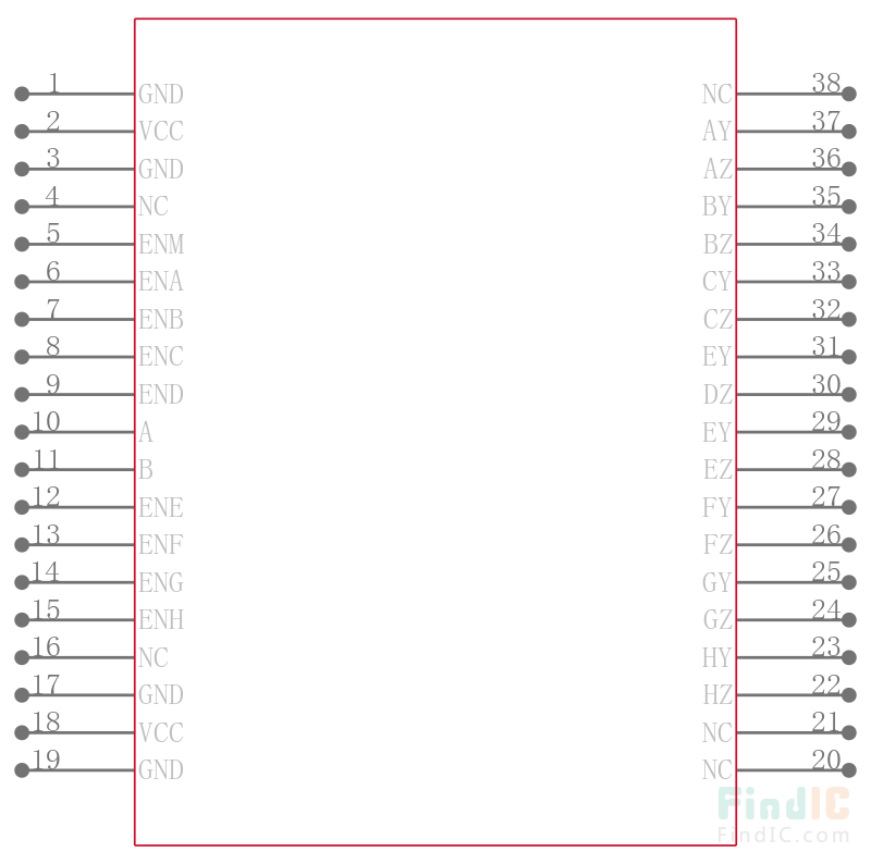
SN65LVDS108DBTR 引脚图
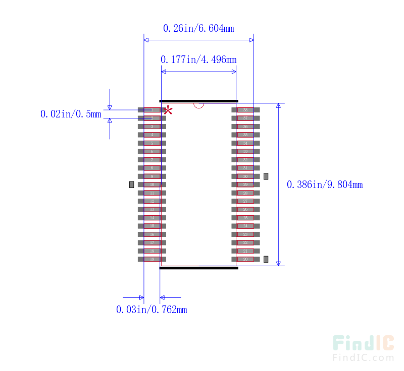
SN65LVDS108DBTR 封装图
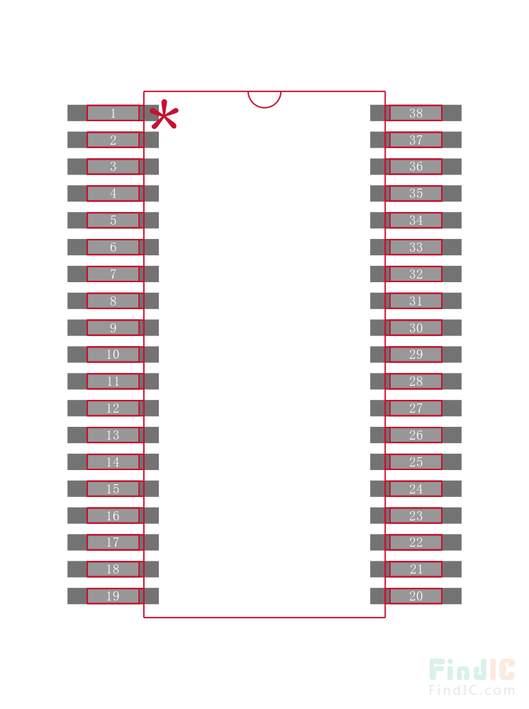
SN65LVDS108DBTR 封装焊盘图
产品概述
1:8 LVDS 时钟扇出缓冲器 38-TSSOP -40 to 85
DESCRIPTION
The SN65LVDS108 is configured as one differential line receiver connected to eight differential line drivers. Individual output enables are provided for each output and an additional enable is provided for all outputs. The line receivers and line drivers implement the electrical characteristics of low-voltage differential signaling (LVDS). LVDS, as specified in EIA/TIA-644, is a data signaling technique that offers low power, low noise emission, high noise immunity, and high switching speeds. (Note: The ultimate rate and distance of data transfer is dependent upon the attenuation characteristics of the media, the noise coupling to the environment, and othersystem characteristics.)
FEATURES
• One Line Receiver and Eight Line Drivers Configured as an 8-Port LVDS Repeater
• Line Receiver and Line Drivers Meet or Exceed the Requirements of ANSI EIA/TIA-644 Standard
• Typical Data Signaling Rates to 400 Mbps or Clock Frequencies to 400 MHz
• Enabling Logic Allows Individual Control of Each Driver Output, Plus All Outputs
• Low-Voltage Differential Signaling With Typical Output Voltage of 350 mV and a 100-Ω Load
• Electrically Compatible With LVDS, PECL, LVPECL, LVTTL, LVCMOS, GTL, BTL, CTT, SSTL, or HSTL Outputs With External Termination Networks
• Propagation Delay Times < 4.7 ns
• Output Skew Less Than 300 ps and Part-to-Part Skew Less Than 1.5 ns
• Total Power Dissipation at 200 MHz Typically Less Than 330 mW With 8 Channels Enabled
• Driver Outputs or Receiver Input Equals High Impedance When Disabled or With VCC < 1.5 V
• Bus-Pin ESD Protection Exceeds 12 kV
• Packaged in Thin Shrink Small-Outline Package With 20-Mil Terminal Pitch
