LF253DT点击型号即可查看芯片规格书
LF253DT 中文资料规格参数
| 技术参数 | 供电电流 | 1.4 mA |
电路数 | 2 | |
通道数 | 2 | |
针脚数 | 8 | |
耗散功率 | 0.68 W | |
共模抑制比 | 70 dB | |
带宽 | 4 MHz | |
转换速率 | 16.0 V/μs | |
增益频宽积 | 4 MHz | |
输入补偿电压 | 3 mV | |
输入偏置电流 | 20 pA | |
工作温度(Max) | 105 ℃ | |
工作温度(Min) | -40 ℃ | |
增益带宽 | 4 MHz | |
耗散功率(Max) | 680 mW | |
共模抑制比(Min) | 70 dB | |
电源电压 | 6V ~ 36V | |
| 封装参数 | 安装方式 | Surface Mount |
引脚数 | 8 | |
封装 | SOIC-8 | |
| 外形尺寸 | 宽度 | 4 mm |
封装 | SOIC-8 | |
| 物理参数 | 工作温度 | -40℃ ~ 105℃ |
| 其他 | 产品生命周期 | Active |
包装方式 | Tape & Reel (TR) | |
| 符合标准 | RoHS标准 | RoHS Compliant |
含铅标准 | Lead Free | |
| 海关信息 | ECCN代码 | EAR99 |
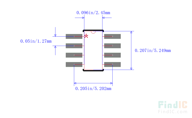
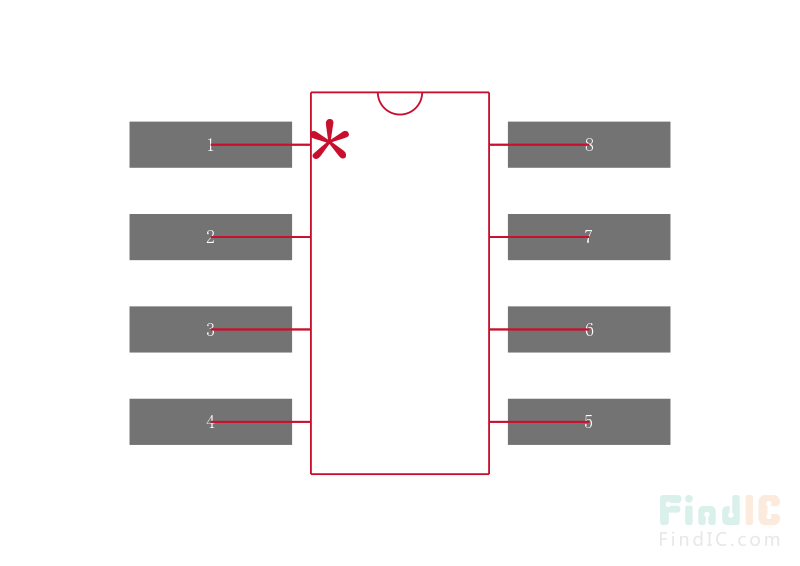
LF253DT 引脚图 | 封装图 | 封装焊盘图
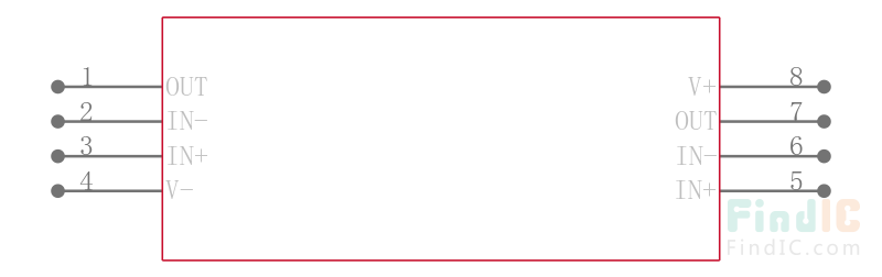
LF253DT 引脚图
LF253DT 封装图
LF253DT 封装焊盘图
产品概述
LF253 SOP8 宽带宽 双通道 J-FET 运算放大器
These circuits are high speed JFET input dual operational amplifiers incorporating well matched, high voltage JFET and bipolar transistors in a monolithic integrated circuit.
The devices feature high slew rates, low input bias and offset currents, and low offset voltage temperature coefficient.
**Key Features**
.Latch up free operation
.Internal frequency compensation
.Low power consumption
.Low input bias and offset current
.Wide common-mode (up to VCC +) and differential voltage range
.High input impedance JFET input stage
.High slew rate 16 V/µs (typical)
.Output short-circuit protection
